In recent years, with the rapid development of the electronics industry, miniaturization design is more and more widely used, and SIP technology is also a term often heard in the industry. With the chip technology gradually reaching the limit, more and more companies will bring forth new ideas in packaging technology, and unlimited potential has emerged in electronic packaging design.
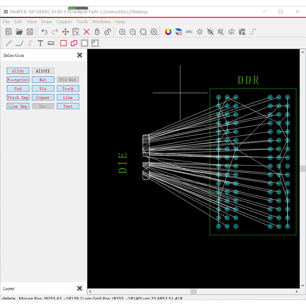
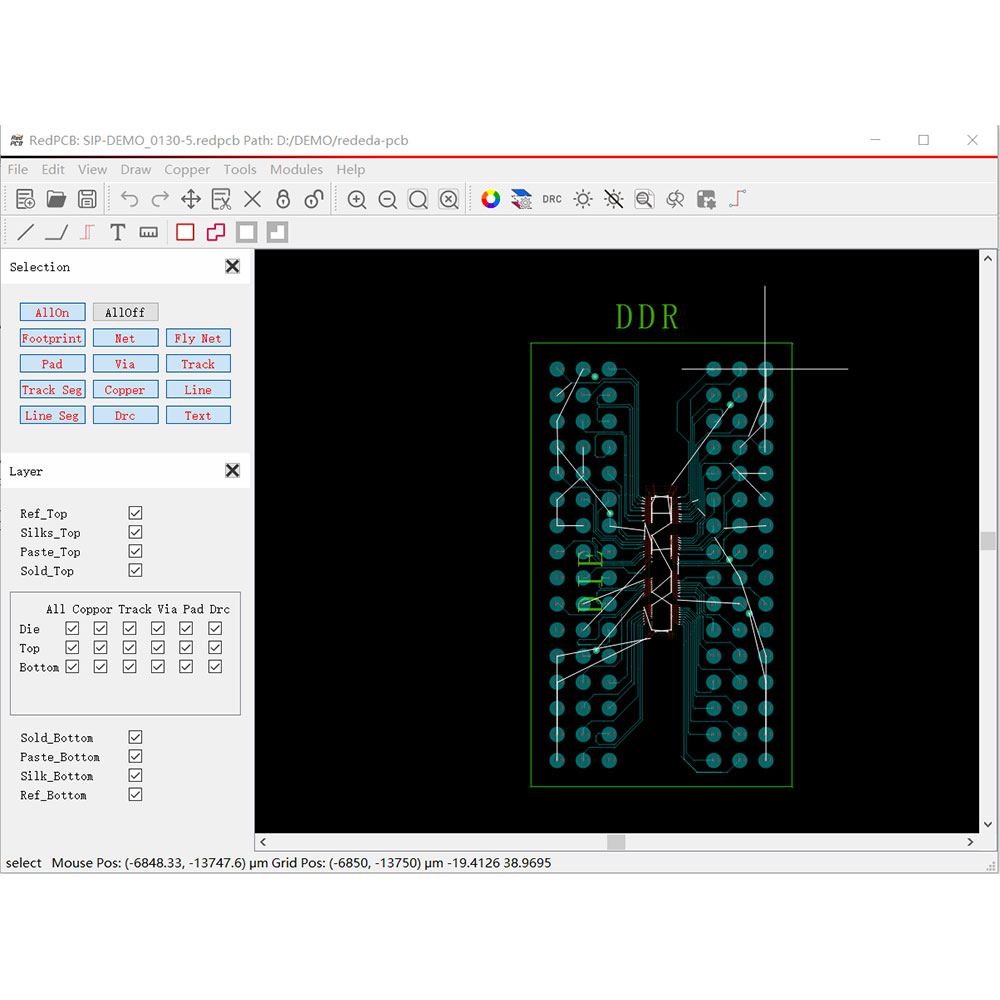
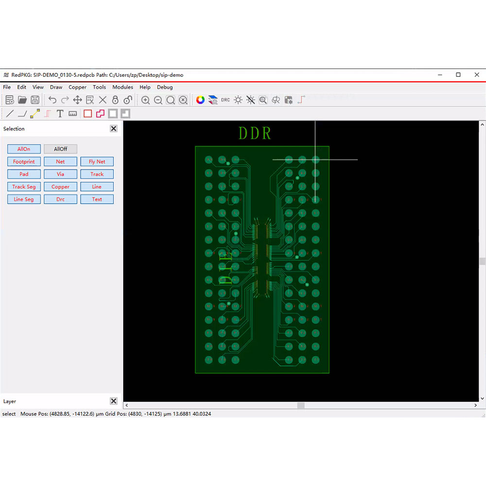
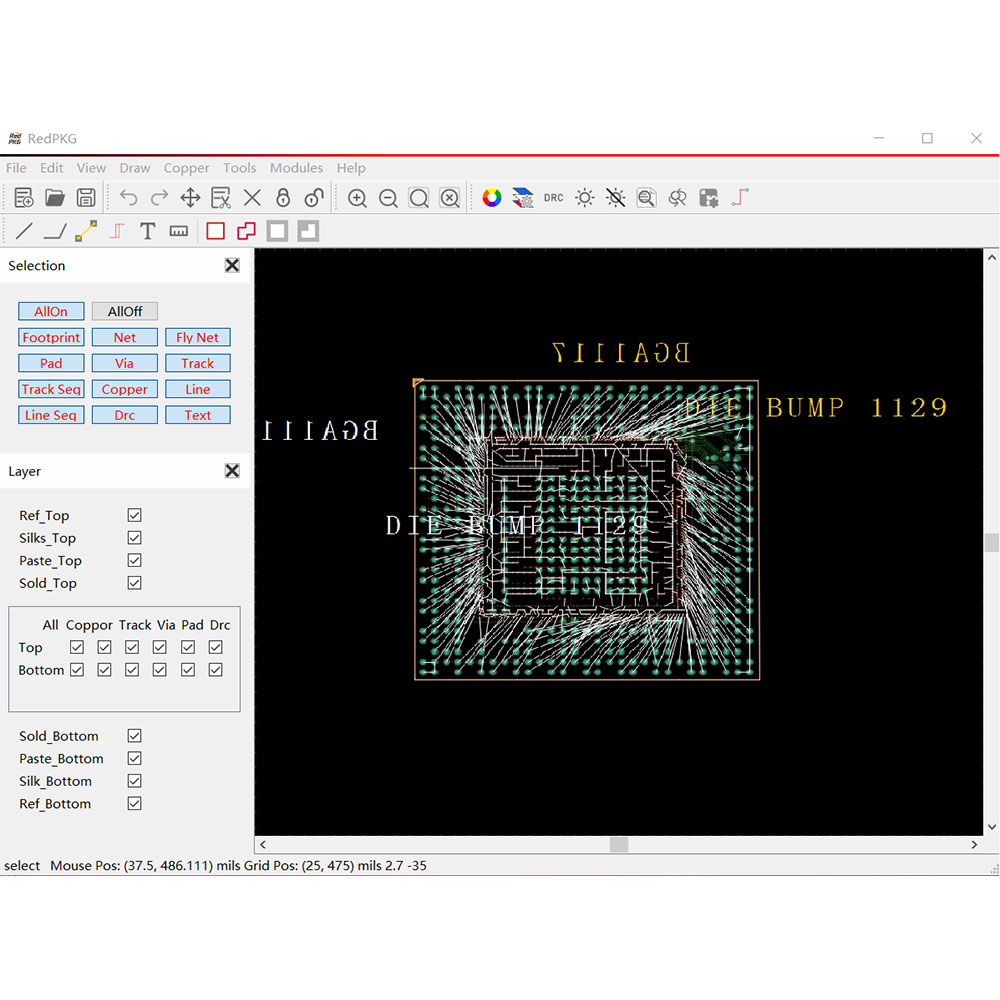
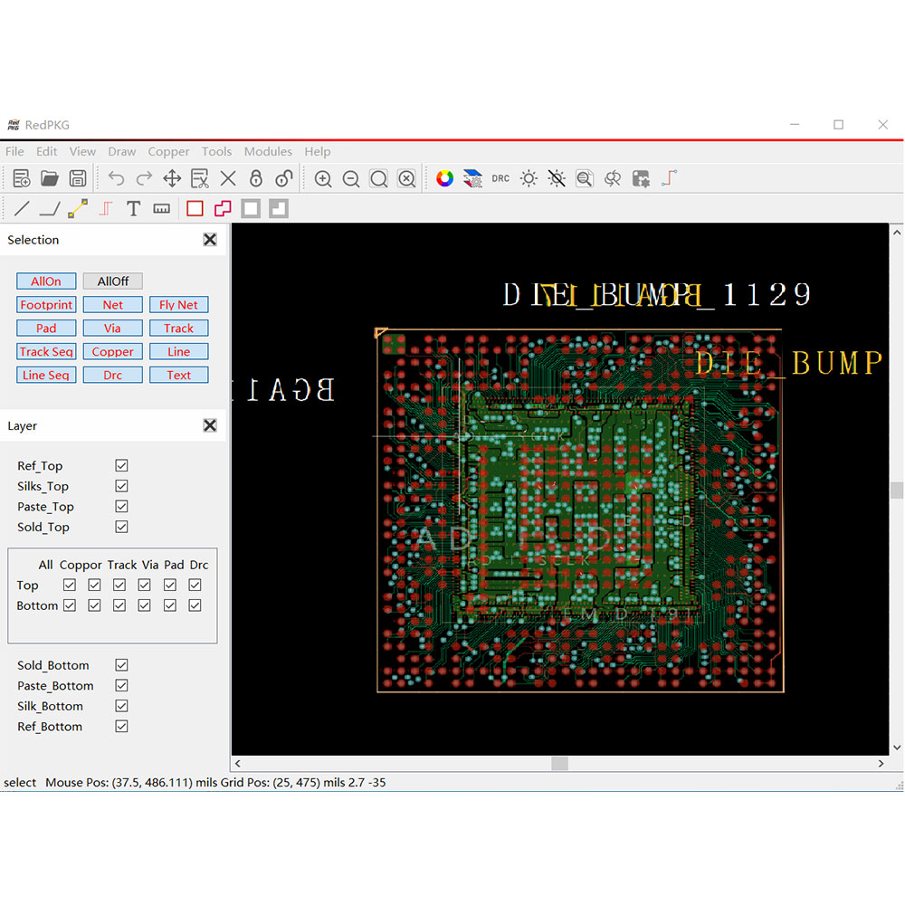
RedPKG is a chip package design tool under RedEDA platform, which provides PKG process design including DIE PAD parameter setting, Ball parameter setting, Net In import, layout, routing, machining data output and so on. It can satisfy the design of FC, WB and other types of packaging for users. It is applied to the field of IC design and production, such as chip development and package design, and provides a full process platform of theoretical design and physical design for IC design users in the packaging stage.

● Support RedPKG with Excel table import mode, quickly complete the Pin Map mapping of Die and Package.
● The overall design interface of RedPKG is simple, which makes it easier for engineers to use.
● Supports encapsulation design of Wire Bonding and Flip Chip types.
● Fine cascading management and color manager make efficient design within reach.
● Generate DIE encapsulation directly according to DIE information table
● Generate BALL encapsulation directly according to BALL information table
● Generate CSV Netlist NET IN according to Pin Mapping
● Package's powerful hollowing out and transparent display.